8085 microprocessor
As previously mentioned, Intel introduced 8085 microprocessors in 1976.The intel 8085 is one of the most popular 8 bit microprocessor.The 8085 microprocessor consists of three main sections i.e. Arithmatic and logic unit, A timing control unit and several registers .The 8085 microprocessor is a microprocessor update of 8080. The 8080 processor has been updated to the 8085 microprocessor by enabling / disabling instruction pins and interrupting pins. Let us Discuss the 8085 microprocessor architecture in detail.

8085 microprocessor.
Characteristics 8085 microprocessor
A 8-bit microprocessor with 40-pin dual line packaging is 8085 micro-processor. In this processor, the address and data bus are multiplexed, which helps to give more control signals. 8085 has one non-maskable interrupt and three maskable interrupts. The serial interface provides serial input data (SID) and serial output data (SOD).
The 8085 microprocessor's configurations include mainly the 8-bit data bus, 16-bit address bus, 16-bit program counter, 16-bit stack pointer, 8-bit Registers, + 5V voltage electric supply and a 3-2MHz single-segment CLK system.
Microwave ovens, washing machines, gadgets and so on are used on 8085 microprocessors.
The next updated version of 8085 is 8085A which is given in this image.

8085 microprocessor.
Architecture of the 8085 Microprocessor
Architecture of the 8085 Microprocessor
8085 microprocessor architecture includes mainly a time and control unit, a logical and arithmetic unit, decoder, instruction register register, interrupt control, register array, serial I / O control. The central processing unit is the most important part of the microprocessor.

8085 microprocessor.
Arithmetic as well as logical is the key operation of ALU that consists of addition, increment, subtraction, decrement, logical actions like AND, OR, Ex-OR, supplement, evaluation, left or right shift. Both temporary registers and accumulators are used to maintain the information during the transactions, so the result is stored inside the accumulator. The various flags are arranged or rearranged according to the results of the operation.
Arithmetic and Logic Unit
Arithmetical work such as+,-,*, / and logical operations such as AND and OR, NOT etc are always necessary. There is also a need to create a separate unit that can carry out such operations. The Arithmetical and Logic Unit (ALU) conducts these operations. ALU carries out these 8-bit data operations.

8085 microprocessor.
However, these operations can not be carried out without the use of input (or) data to perform the desired operation. So where do the ALU come from these inputs? Accumulator is used for this purpose. ALU receives its accumulator and temporary register information. The result will be stored in the accumulator after processing the necessary operations.
Timing and control unit
It provides the microprocessor with a timing and control signal for operation. The time and control signals that control external and internal circuits are shown below
1.RESET Signals: RESET IN, RESET OUT.
2.DMA Signals: HOLD, HLDA.
3.Status Signals: S0, S1, IO/M’.
4.Control Signals: READY, RD’, WR’, ALE.
2.DMA Signals: HOLD, HLDA.
3.Status Signals: S0, S1, IO/M’.
4.Control Signals: READY, RD’, WR’, ALE.
Accumulator
Accumulator is nothing but an 8-bit register. Accumulator helps two quantities to be stored. The processing data is stored in the accumulator via the arithmetic and logic unit.
The results of the Arithmetic and Logic unit operation are also stored. The accumulator is also referred to as an 8-bit register. The accumulator is connected to the ALU (Arithmetical and Logic Unit) and the internal data bus.
It is possible to send or receive data from the Interior Data Bus using the accumulator.
General Purpose Registers
Besides the 8085 accumulator, there are six special register types known as General purpose. registers. These registers for general purposes are used to keep data as any other register. The registers for general use are B, C, D, E, H and L for 8085 processors.
They can be hold 8-bit data in each register. These registers can be used in pairs to hold 16-bit data, in addition to the above function. It is possible to store 16-bit data in pairs such as B-C, D-E and H-L. The H-L pair is a memory indicator.A memory indicator contains a specific memory location's address. You can store 16-bit when you work together.
Program Counter
A special purpose register is a program counter. Consider that the processor performs an instruction. Once the ALU has completed the execution of the instruction, the processor will search for the next instruction. There is a need to hold the address of the next instruction to be executed in order to save time. The program counter takes care of this.
A counter program stores the address of the next instruction. In other words, the counter tracks the memory address of the instructions performed by the microprocessor and the memory address of the following instructions.
When a instruction is executed, the microprocessor increases the program so that the program counter points towards the next instruction's memory address. A program counter is 16-bit registor .
Stack Pointer
The Stack Pointer is a 16-bit register used as a memory pointer. A stack is only the random access memory area.
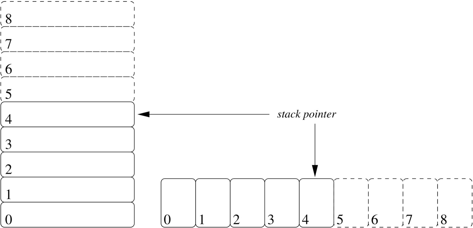
Stack Pointer contains the address of the top of a stack. In these programs a set of instructions, excluding stack transactions, is stored in the stack pointer register.
Temporary register
It is an 8-bit register containing temporary arithmetic and logical data.
Increment or Decrement Register
The content of the 8-bit register or a memory position can be increased by one. The 16-bit register is useful to increase or decrease program counters and to record content with a stack pointer. This operation can be conducted at any memory or register position.
Flag register
It is an 8-bit register with five 1-bit flip-flops, which is supported by either 0 or 1 depending on the accumulator result. This is the set of 5 flip-flops: Sign (S), Zero (Z), Auxiliary Carry (AC), Parity(P),Carry(C).
Instruction register and decoder
The register is 8-bit. If a instruction is fetched from the memory, it's saved in the instruction record. Instruction decoder decodes information in the Register of Directives.
Serial Input/output control
It controls the communication of serial data using both these instructions: SID (Serial input data) and SOD (Serial output data).
Interrupt control
As the name implies, the interrupts are controls during a process. If a microprocessor executes a main program and if an interrupt occurs, the microprocessor moves the control from the main program to process the input application. The check goes back to the main program after the request has been completed.
The 8085 microprocessor has five interruption signals: INTR,INTA, RST 7.5, RST 6.5, RST 5.5, TRAP.
Address buffer and address-data buffer
In the address buffer and the address data buffer the content stored in the stack pointer and program counter is loaded to communicate with the CPU. These Busses have memory and I / O chips connected and the CPU can exchange the desired data with the memory and I / O chips.
Address bus and data bus
The Data Bus transmits the storage data. It is two-way, whereas the address bus transports the place to where it should be stored. The data & address I / O devices are transferred.
Thank you so much for reading the 8085 microprocessor.

Here, you shared the most valuable post. I'm really happy to read this. Thank you.
ReplyDeleteJMeter Training in Chennai
learn JMeter
JMeter Course
JMeter Training in OMR
Appium Training in Chennai
javascript training in chennai
core java training in chennai
C C++ Training in Chennai
I would definitely thank the admin of this blog for sharing this information with us. Waiting for more updates from this blog admin.
ReplyDeletegst training in chennai
Angularjs Training in Chennai
CCNA Training in Chennai
salesforce training institute in chennai
ui design course in chennai
شركة مكافحة حشرات بتبوك
ReplyDeleteشركة مكافحة حشرات بضباء
شركة مكافحة حشرات ببريدة
شركة مكافحة حشرات بأبها
شركة مكافحة حشرات بخميس
شركة مكافحة حشرات بجده
Nice blog!! I hope you will share more information like this. This will be more useful for my studies and research.
ReplyDeleteangular js training in chennai
angular js online training in chennai
angular js training in bangalore
angular js training in hyderabad
angular js training in coimbatore
angular js training
angular js online training